 Рус
Рус
 Site map
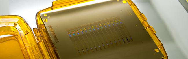
Shared Use Centre Photomask
Design and Manufacture
Design and Manufacture


The aspects of the specialized radiation-resistant VLSI design based on heterostructures

The 9th Scientific and Practical Conference ‘The aspects of the specialized radiation-resistant VLSI design based on heterostructures’ took place in Nizhny Novgorod in February 2009. At the conference the specialists of the center made a speech ‘The peculiarities of the development and technical renovation of the center fabricating photomasks for the integrated circuits of 0.18 micrometer design rule’.
The modern innovative infrastructure


Use of the modern equipment at all production phases


Our partners


SCPDM
© 2008-2015 Contacts
+7 (499) 720-69-67
© 2008-2015
Contacts
+7 (499) 720-69-67